13 Jul Light emitting diodes – LEDs | How they work and their limited use in optical networking
Light emitting diodes (LEDs) have seen an explosive growth in multiple industries, including home lighting, displays and TV and smartphone backlighting. However, despite their widespread use in early optical communication systems, LEDs currently represent a small part of the communication light source market. The emergency of vertical-cavity surface-emitting lasers (VCSELs) which offer better performance and cost significantly less than other laser diodes is further eroding the communication light emitting diode market.
Notwithstanding their limited use in optical networking, understanding how LEDs work is the basis for understanding semiconductor laser diodes used in all segments of the optical communication networks. Moreover, understanding the PN-junction, the underlying concept behind the LED (or any diode for that matter), is the basis for understanding many other concepts in information and communication technologies – from basic electronics to such advanced topics as Silicon photonics. This article covers the fundamentals of the PN-junction and the LED with reference to its application in optical communications.
The PN-junction
A PN-junction is created by fusing P-type and N-type semiconductor materials together. But before we look at what happens when such materials are brought together, let us digress and look at the formation of P-type and N-type materials in a Silicon crystal. Although Silicon itself is not used as the main material in LEDs as explained later, understanding the Silicon semiconductor is a good starting point to understanding the PN-junction.
The atomic number of Silicon is 14 and has 14 electrons arranged in several orbitals with 2 electrons, 8 electrons and 4 electrons as shown below.
![]()
But for understanding the crystalline nature of Silicon and how P-type and N-type materials are formed, we are more interested in the number of electrons in the outermost shell or the valence electrons. Like all group 14 elements such as Carbon (C) and Germanium (Ge), Silicon has 4 valence electrons. In other words, Silicon is tetravalent.
Silicon is found in nature in the form of Silica or Silicon Dioxide (SiO2). In fact, inland continental, and non-tropical coastal sand consists mostly of Silica. While pure Silica is used to manufacture the glass component of an optical fiber, in electronics pure Silicon (Si) is used. SiO2 must be reduced, or have oxygen removed from it to form Silicon crystals.
The figure below depicts a Silicon crystal. Each atom of the crystal forms covalent bonds with its nearest neighbors. In a covalent bond, atoms share their electrons with two adjacent atoms, each sharing one electron. Of course, covalent bonding differs from ionic bonding where an atom transfers an electron to another atom or receives an electron from another atom.
![]()
To make a P-type material, Silicon is doped with a trivalent (with three valence electrons犀利士
) material, such as Boron. The doping process involves replacing some of the Silicon atoms with the dopant atoms, Boron in this case (see figure below). The introduction of the Boron atom destabilizes the crystal structure of Silicon. There is now a deficiency of an electron where the Boron atom is attached. Such an absence of an electron is referred to as a hole and a semi-conductor material with holes is a P-type material.
If the Silicon crystal is doped with a pentavalent material (with five outermost electrons) such as phosphorous, the opposite happens. Instead of a hole, an extra electron is introduced where the Phosphorous atom is attached. Semiconductor materials with excess electrons are N-type semiconductor materials.
![]()
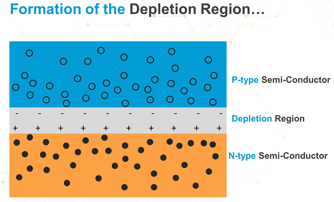
Now, consider what happens when the N-type and P-type materials are fused together to form the PN-junction. Some of the electrons from the N-type material, near the junction, diffuse across the junction and combine with the holes on the P-type side. The migration of electrons across the junction is equivalent to holes crossing in the opposite direction. Note that, while the holes in the P-type material and the excess electrons in the N-type material destabilize the crystal structure, the dopant atoms are neutral because they have the same number of electrons as protons. But when an electron combines with a hole on the P-type side, it results in a negative ion leaving the P-type material near the junction with a net negative charge (see figure below).
On the other hand, by leaving the N-type material, electrons leave a net positive charge. The process continues until there is equilibrium and no more electrons can cross the junction. This is because the negative charge on the P-type side repels any more electrons that try to cross the junction. Similarly, the positive charge on the N-side repels any more holes trying to cross to the N-side. This results in a potential barrier known as the depletion region because it is devoid of any holes or electrons.
An important aspect of the barrier is that it is possible for electrons to cross it if they can gain some extra energy. Such extra energy can be supplied to the electrons in the form of an appropriately biased voltage, as describe in the next paragraphs.

Biasing the PN-junction
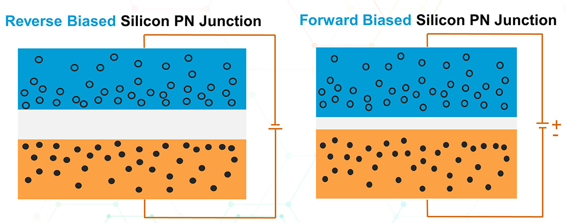
If a reverse bias DC voltage is applied to the PN-junction by connecting the positive terminal of a DC source to the N-type material and vice versa, the effect is to enlarge the depletion region and make it even harder for electrons to cross the junction. This is because the applied voltage tends to force electrons away from the depletion region towards the N-type material and vice versa. No current will flow in the circuit under this scenario.
However, if a forward bias DC voltage with the positive terminal connected to the P-type material and the negative terminal to the N-type material is applied, an electric current will flow in the circuit. In this scenario, electrons are being pushed towards the P-type side of the depletion region and vice-versa. Because the electric voltage has supplied more energy to electrons in a way that gives them a push, they can easily cross the barrier to get to the P-side while holes drift in the opposite direction. In other words, the applied voltage shrinks the depletion region and makes it easier for electrons to cross.
Thus far, we have established that a diode can only allow current to flow in one direction prohibit it from flowing in the other direction. This is an important feature of semiconductor technology.

More importantly, forward biasing results in electrons and holes combining in the depletion region to give out energy. However, when the semiconductor material used is Silicon, the energy emitted is in the form of phonons, where a phonon is a unit of sound. While phonons are very interesting, they are irrelevant for our discussion because our focus is on photonics and we are interested in the emission of photons – a photon being a unit of light.
Compound semiconductors and light emission
When a suitable compound semiconductor material is used, light is emitted during the hole-electron combination process.
Group 13 and Group 15 elements can be combined to form important compound semiconductor materials (or Group 13-15 compound semiconductors) that can convert electric energy into light energy. Group 13 elements used include Aluminum (Al), Gallium (Ga) and Indium (In) while some of their important Group 15 counterparts include Phosphorous (P) and Arsenic (As). The compound semiconductors are doped with suitable materials to either create holes or electrons as described before. To create an N-type material from Gallium Arsenide (GaAs) for example, Silicon is used as the dopant material while Group 2 elements such as Beryllium (Be) or magnesium (Mg) are used as the dopant to create the P-type material.
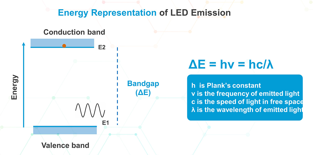
The photon or light emission from these compound semi-conductor PN-junctions during electron hole combination is more conveniently described using the energy levels of the electrons. When energy is supplied to an electron, it can be excited and can jump from the valence band to the conduction band which is at a higher energy level. At this energy level, an electron can move freely in the material and when it falls back to the valence band it releases energy equal to the energy difference between the bands, as illustrated below.

A very important aspect of this energy is that it is proportional to the frequency of the released photon and can be expressed by the equation:
ΔE = hν = hC/λ, where h is the Plank’s constant, ν is the frequency of the light, C is the speed of light in vacuum and λ is the wavelength of the light.
Back in 1977 when GT&E and AT&T sent live telephone signals over a 9km of fiber optic cable at 6Mbps, the system was operating at the 850nm wavelength band. This wavelength corresponds to the bandgap of GaAs which was a well-known emitter of infrared radiation for a long time. The 850nm wavelength band is still commonly used for short reach communication applications such as in premises and data center networks. We can show how the wavelength is calculated from the bandgap using the photon energy equation above.
The bandgap of GaAs at room temperature is 1.42eV or 2.28 x 10⁻¹⁹J. The Plank’s constant is about 6.6×10⁻³⁴J.S and C is about 3×10⁸m/s. By substituting these values in the photon energy equation, we end up with:
2.28×10⁻¹⁹J = (6.626176×10⁻³⁴J.S)(2.99792458×10⁸m/s)/λ
This results in λ = 8.73×10⁻⁷m or about 870nm which is within the 850nm band. Additional variables, such as dopant concentration and temperature can be adjusted to target specific wavelengths within the band. The most important take-away here is that the wavelength of the LED is dictated by the semiconductor material used.
The table below shows common semiconductor materials, their bandgaps, and corresponding wavelengths.
The use of InGaAsP, for example, enables 1300nm wavelength which is a common LED wavelength for short reach applications especially when chromatic dispersion is an important consideration. Chromatic dispersion is discussed in detail in the OTT CONA course. InGaAsP is also used in laser diodes for a wide range of wavelengths, including around the optical C-band (1530nm-1570nm) where most optical networking systems operate.
Important properties of communication light emitting diode
Non collimated light– LED light is not collimated which means that light waves travel in different directions. As a result, the beam radius can undergo significant increase, or divergence, after travelling for a short distance. This makes focusing LED beam into a small optical fiber core a challenge. As a result, multimode optical fiber, with a significantly larger core than single mode fiber, is used with LED light sources.
Incoherent light – LED light is incoherent which means that the phase difference between waves is not constant over time. The waves on the left side of the figure below are incoherent. Although they all start at the same relative position, at maximum amplitude and in phase or with a zero-phase difference between them, by the time they get to the end they are no longer in phase. Therefore, their phase difference is not constant, it changes over time. On the contrary, the waves on the right all start in phase and end up in phase. The phase difference between them has not changed. Note that even if they started out of phase, as long as their phase difference remains the same, they will be coherent.

Wide spectrum – LED light has a wide spectral width where spectral width is the distribution of emitted power as a function of wavelength. A wide spectral width implies that a wide range of wavelengths around the center wavelength is emitted, making the system more susceptible to chromatic dispersion and other fiber impairments. In an ideal world, a perfect communication line spectrum will be a line with all the light power concentrated in one wavelength. However, in a real world any light source will have a line width greater than zero. As will be discussed in subsequent articles, laser sources have much narrower spectral widths than LEDs.
Low modulation – LEDs cannot be modulated fast enough to support higher data rates. LEDs are therefore typically used for lower data rate applications.
Low cost – LEDs are inexpensive and this is the main reason why they are still in use. It also explains why multimode fiber which is significantly more expensive than standard single mode fiber is used in short reach applications in which large numbers of transmitter/receiver pairs are used. With multimode fiber, one can use lower cost LEDs (or VCSELs) and significantly lower the overall cost of the network infrastructure.
Summary
In summary, light emitting diodes are widely used in multiple industries but their use in optical communications is limited. They are mostly used in short distance applications at relatively lower transmission rates. The operation of the LED is based on the PN-junction of compound semiconductor materials such as GaAs. The basic operation of the LED is similar to that of the laser diode, which is basically an enhancement of the LED. Finally, the wavelength of a diode depends on the bandgap of the semiconductor material used.
Founder and Technical Director at FiberGuide, Lecturer, Scientist and Engineer. Passionate about optical networking and information and communication technologies. Connect with me on Linkedin – https://www.linkedin.com/in/jabulani-dhliwayo-1570b5b


Sorry, the comment form is closed at this time.